|
High-efficiency photo-electron conversion devices |
|||||
High-efficiency photo-electron conversion devices Semiconductor processes and nanofabrication Characterizations and applications of nanomaterials Optical characterization of graphene Graphene-gold oxide photodetector Optical analysis of hollow gold nanoparticles Photomodification of hollow gold nanoparticles for high-density data storage Light harvesting and light extraction Light extraction efficiency of LEDs Antireflection structures for solar cells Optical analysis techniques Eco-friendly devices and sensors
|
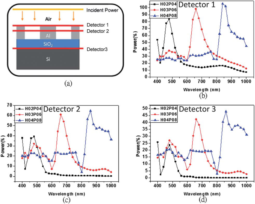
Optimizing surface plasmon resonance effects on finger electrodes to enhance the efficiency of silicon-based solar cells In this paper we demonstrate a technique for improving the conversion efficiency in conventional silicon |
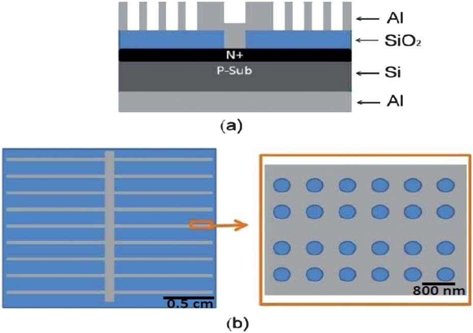
Schematic representation of a tested device. (a) Cross-sectional view of a device featuring a metal hole array, for the SPR effect, on the Al electrode. (b) Top view of a device for mimicking a conventional solar cell; (left) the opaque metal finger electrodes are colored gray; expanded inset (right): design of the electrode for the suggested SPR effect.
|
|||
Copyright(c) 2008 Nano-optpelectronics Lab., Department of Material Science and Engineering, National Taiwan University No. 1, Sec. 4, Roosevelt Road, Taipei, 10617 Taiwan(R.O.C) Phone:+886-2-3366-3240 Fax:+886-2-2362-7651 |
|||||